Quick Overview: Multidisciplinary product creation powered by your unconstrained network. Work concurrently across design, sourcing, and ... Click to join the free 6-layer PCB prototyping program, leave your contact info, and get ... jlcpcb vias design PCB Fab & Assembly from $2! Register to get $60 Coupons:
Via In Pad Reliability When - Detailed Overview & Context
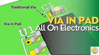
Multidisciplinary product creation powered by your unconstrained network. Work concurrently across design, sourcing, and ... Click to join the free 6-layer PCB prototyping program, leave your contact info, and get ... jlcpcb vias design PCB Fab & Assembly from $2! Register to get $60 Coupons: Due to an error I had previously made in a design, I wanted to share the correct method to placing a Visit to try the application. No installation is required. Show your support PCB ... Basics, guidelines, and best practices for vias in PCB designs. From sizing, to placement, to transfer and stitching vias, and more!
Grab your free Design Mistakes Checklist Bundle: ... About this video: Take your PCB designs to the next level with JLCPCB's advanced 6-layer PCBs! Featuring In this video, we walk through a detailed BGA Learn how PADS Professional enables you to quickly and efficiency optimize routing channels by simplifying the use of blind and ...