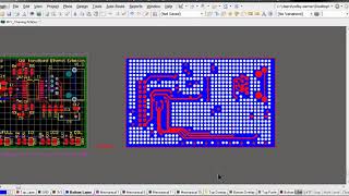
Quick Overview: Multidisciplinary product creation powered by your unconstrained network. Work concurrently across design, sourcing, and ... First we will create a dummy net to assign the polygons we're going to create we will need this in order for the Basics, guidelines, and best practices for
Stitching Via Deep Dive Pcb - Detailed Overview & Context
Multidisciplinary product creation powered by your unconstrained network. Work concurrently across design, sourcing, and ... First we will create a dummy net to assign the polygons we're going to create we will need this in order for the Basics, guidelines, and best practices for Watch this animation to understand better how a signal is lost when travelling If you have attended our webinars in the past, we are always pressed to keep the presentations under an hour. With any given ... In this video, Zach Peterson explains why differential